Measuring 1024 quantum dots in 5 minutes: How our diverse team collaborates to deliver world-leading results
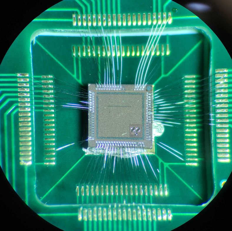
In a major step forward for mass characterisation of quantum devices made on a silicon chip our team has demonstrated how 1024 quantum dots, fabricated in a commercial semiconductor foundry and occupying an area of less than 0.1mm² can be measured in less than 5 minutes. This is at least 100 times faster than the state of the art, which can take 24 hours or longer to read the equivalent number of dots.
You can read more about the result in our official press release, but we wanted to also share how our team of engineers and physicists work together to achieve these results. So, follow us on a journey as we map out how we get from chip design to measurement result.
Designing Bloomsbury
Quantum Motion’s latest chip – called Bloomsbury – is a 3×3 mm² device created by a tier one foundry using the same mass production processes used in standard electronic chip manufacturing. But unlike regular computer chips, Bloomsbury contains thousands of quantum dots into which single electrons can be loaded, one by one, to serve as qubits.
 “The design of Bloomsbury was challenging,” said Alberto Gómez Saiz, IC lead at Quantum Motion. “We were a new team when we started taping-out, not even six months old, and we were in the middle of the covid pandemic making it more difficult to achieve in-person collaboration with our quantum hardware team, which is essential for good design.”
“Bloomsbury combines quantum structures together with conventional electronics capable of working at cryogenic temperatures with a very low power budget. This is a first for our IC team: we designed the multiplexer, we co-designed the quantum structures, and we integrated it all together along with digital electronics to create a large-scale system.”
“The resulting fast mass characterisation of devices demonstrates that our work can lead to a reliable product. We have transitioned away from characterising one device, examining a once in a best-case scenario, to doing it repeatedly on a large scale with many devices.”
“This work shows that the step of gathering data is no longer the bottleneck in the research process, and this fast characterisation will play a key role in optimising the designs of our quantum processors.”
Validating Bloomsbury
After the chip design is finalised and sent off for fabrication, the IC validation team start preparing for mass characterisation.
 Grayson Noah, Senior IC Validation Engineer at Quantum Motion, said: “The chip design was finalised at the start of the year, so our team knew what was going to be on the chip and we could start preparing the hardware and software needed to test it.”
“It is a big challenge to characterise this many quantum devices. We need to be able to select different quantum dot structures, rapidly switch between them, and conduct both DC and AC measurements on each individual device when it is selected through a multiplexer.”
“In those few months, while the chip was being fabricated, the IC validation team was putting together documentation, software to help automate testing, and advising on best practice for how to test a lot of chip circuitry quickly.”
“What our IC validation team brings to the table is experience in high volume testing. In a production environment or other traditional electronics testing, test time is one of the biggest manufacturing costs for a company that is trying to produce high volume products. Our team has knowledge of test time reduction techniques that helps us minimise the time it takes to test a large quantity of devices.”
Measuring Bloomsbury
“This set of measurements was the main project for my internship this summer at Quantum Motion,” said Domenic Prete, Quantum Motion Hardware Intern who is currently a PhD candidate at Scuola Normale Superiore di Pisa.
 “It is an amazing opportunity for me to work in an excellent environment with top people from the field. I was hoping to work on a project like this when I joined, but I didn’t imagine that such an advanced device could exist!”
“We started by bonding up the brand-new Bloomsbury chips to our PCBs, which were designed by James Kirkman in our IC team. The first challenge for us was to confirm that we could perform radiofrequency reflectometry measurements on the Bloomsbury chip. This is a key ingredient in being able to measure devices at high speed with good signal-to-noise, and allows you to study a wider range of quantum dot designs. We had to show that the advanced analogue and digital electronics in Bloomsbury that allows you to manipulate and select many quantum devices was able to handle these high frequencies well, even at low temperatures.”
“In my experience as a student in an academic lab, you usually address these devices individually, which means you need approximately six wires to measure your single quantum device. Obviously when you are trying to measure the thousands of devices that we have in Bloomsbury, this is not possible. For this you need some on-chip electronics, which the IC team developed and designed – what they achieved here seems super complex to me! This was ultimately what allowed us in the quantum hardware team to perform and achieve this brilliant result!”
 Mark Johnson, Senior Quantum Engineer said: “The prior work completed by the IC team really helped us in the quantum hardware team. We could rely on tools that they had created, and if we had any questions on how something worked, they would immediately know.”
“I didn’t expect everything to work as well as it did in the end, there were struggles along the way, but working with such a diverse team who have a wealth of experience and knowledge working with these devices, made the final measurements that much easier!”
“This result shows the huge potential of realising quantum processors using advanced silicon foundry processes. It shows that the approach we are exploring is working, that silicon is a proven platform for quantum computing.”
Beyond Bloomsbury
“We are exploring unchartered territory,” said Alberto Gómez Saiz, IC lead at Quantum Motion, “We are still building knowledge, but this result shows that we have working quality and risk procedures in place that have enabled our ICs to be functional and producing great results on a first design iteration.”
Our team will use the results from Bloomsbury to develop future generations of ICs which integrate prototype quantum processors with digital and analogue electronics. If you want to be part of this revolution in silicon computing take a look at our careers section. We are always looking to speak to talented people – even if we don’t have your dream role listed, please get in touch via jobs@quantummotion.tech.